


Industry News
IQE Releases World's First Commercially Available 200mm (8-inch) VCSEL Wafer
Views : 1570
Update time : 2022-05-20 16:36:00
IQE Corporation announced the launch of the world's first commercial 200mm (8-inch) VCSEL epitaxial wafer. The new epitaxial wafer will benefit foundry partners like silicon-based fabs to achieve silicon and compound integration.
IQE drives the compound semiconductor industry's 200mm diameter epiwafers within the wireless, sensing and display markets.
IQE's 200mm epitaxial wafer will drive compound semiconductor device economic changes, thereby expanding IQE's market influence. the rise in epiwafer diameter will benefit new foundry partners, like silicon-based fabs. More importantly, it makes it possible to integrate compound semiconductors on silicon and apply them to a wider range of devices and applications.
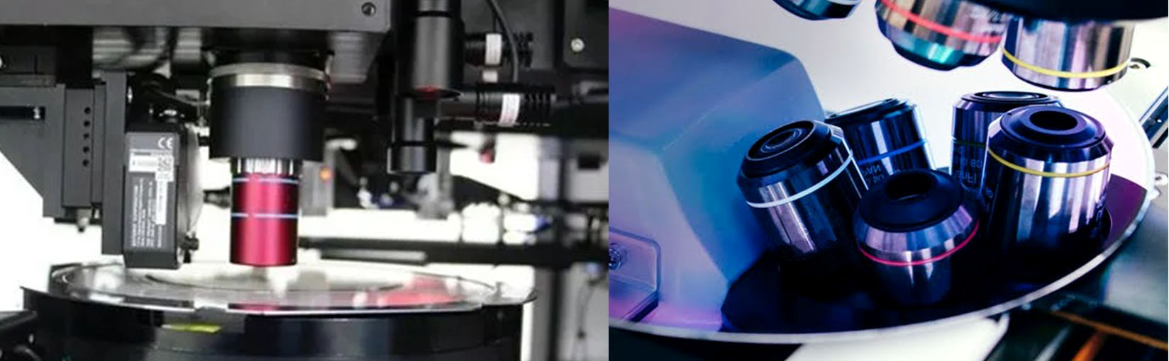
IQE's 200mm VCSEL development is an example of the company's continued innovation and commitment to scaling the wireless and 3D sensing markets. 3D sensing became commercially available with the deployment of high-end smartphones in 2017, when IQE had developed VCSEL epitaxial wafers that scaled from 100mm to 150mm. The introduction of 200mm products will create new opportunities not limited to smartphones, but also include a wider range of smart connected devices and Metaverse applications.
Americo Lemos, CEO of IQE, said: "This is a crucial milestone that positions IQE as a global leader in larger diameter compound semiconductor technology. As stated in our fiscal 2021 results, a key takeaway is that the expansion of our product roadmap. to 200mm, establishing new foundry partnerships to drive business growth. With the explosion of macro trends like 5G and the Metaverse, this advancement will expand the marketplace for wireless and photonics applications and meet the growing demand for compound semiconductors , and can create more value for our technology.”
IQE drives the compound semiconductor industry's 200mm diameter epiwafers within the wireless, sensing and display markets.
IQE's 200mm epitaxial wafer will drive compound semiconductor device economic changes, thereby expanding IQE's market influence. the rise in epiwafer diameter will benefit new foundry partners, like silicon-based fabs. More importantly, it makes it possible to integrate compound semiconductors on silicon and apply them to a wider range of devices and applications.
IQE's 200mm VCSEL development is an example of the company's continued innovation and commitment to scaling the wireless and 3D sensing markets. 3D sensing became commercially available with the deployment of high-end smartphones in 2017, when IQE had developed VCSEL epitaxial wafers that scaled from 100mm to 150mm. The introduction of 200mm products will create new opportunities not limited to smartphones, but also include a wider range of smart connected devices and Metaverse applications.
Americo Lemos, CEO of IQE, said: "This is a crucial milestone that positions IQE as a global leader in larger diameter compound semiconductor technology. As stated in our fiscal 2021 results, a key takeaway is that the expansion of our product roadmap. to 200mm, establishing new foundry partnerships to drive business growth. With the explosion of macro trends like 5G and the Metaverse, this advancement will expand the marketplace for wireless and photonics applications and meet the growing demand for compound semiconductors , and can create more value for our technology.”
Related News
Read More >>
 AI Data Center Optical Evolution: Trends & Market
Sep .20.2026
With the rapid growth of artificial intelligence computing, data centers now need much more bandwidth. The physical limitations of traditional copper cable connections are becoming increasingly apparent as transmission speeds rise.
 The Global OCS Market Will Exceed $8 Billion by 2030
Sep .09.2026
The latest industry forecasts indicate that by 2030, the total size of the global optical path switch market is expected to exceed $8 billion, with a compound annual growth rate (CAGR) of over 30% between 2026 and 2030.
 400G Single-Lane: Next Inflection for AI Datacenters
Aug .27.2026
400G per lane is the next inflection for AI data centers, boosting bandwidth and scaling, but requires advances in materials, packaging, and cooling.
 AI-driven 800G Ramp-up Amplifies Quality Risks
Aug .14.2026
Faced with a surge in orders, leading global manufacturers are increasing production line speeds and shortening delivery cycles. However, the real challenge of this growth goes beyond “can we deliver orders on time?”